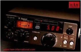
PTBM059COX
|
|
Cybernet PTBM059COX |
|
Retour Accueil RX / TX Viking Puma Multimode Concorde Jumbo Select HandMaster Circuits Cybernet Schémas PTBM094COX PTBM059COX PTBM121D4X PTBM133A4X Manuels Dépannage Circuit BF Driver - PA Alignement PLL Alignement VCO Composants Réparateurs Modifications Beep On/Off Canaux bis SSTV - 14DVK Accessoires / RX Micros Appels sélectifs Antennes Alimentations Fréquencemètres Mesure Century 21D Forum Webmaster Liens utiles
PTBM059COX
maintenance & ADJUSTMENT
The Multimode-II is specifically designed for the environment encountered in mobile use. The use of fully solid-state circuitry and its rugged style result: in high reliability. Should a failure occur, however, replace parts only with identical parts. Do not substitute. (Refer to schematic diagram and part list.)
If the performance described in the owner's manual is not obtained, review the installation section to ensure that the proper procedures were followed. If a problem still exits, refer to the Adjustment procedures in following pages.
circuit description
The transceiver is a 120 channel CB radio which uses a phase locked loop [pll] system of frequency synthesization to produce the crystal controlled channel and IF signal used in operation of the transmitter and receiver sections of the unit. The basic PLL system is comprised of a free-running voltage controlled oscillator (part of IC2), a phase detector, a reference crystal oscillator [Q3] and a programmable divider (IC 1) as seen in diagram below.
The voltage controlled oscillator [VCO] operates in the frequency range of 17.5550 to 18.4450 MHz in the AM/FM/USB mode and 17.5535 to 18.4435 MHz in the LSB mode, and is used to produce two output signals; =1; 37.660 to 39.000 MHz in the AM/FM/USB mode and 37.657 to 38-997 MHz in the LSB mode, =2; at 2.55 to 2.11 MHz. Reference frequency oscillator Q4 oscillates at 10.0525, 10.165, or 10.2775 MHz in accordance with the Band Selector switch (1.5 kHz lower when LSB mode). Its output is fed through the band-pass filter [BPF]/doub!er resulting in an output signal. 20.105, 20.33. or 20.555 MHz in accordance with the band selected (3 kHz lower when LSB mode). This signal beats with the VCO free-running signal producing a 37.66 to 39.0 MHz in the AM/FM/ USB mode and 37.657 to 38.997 MHz in the LSB mode, which is fed to the receiver first mixer [Q22] and also to IC3 (on main circuit board PTBM059), the transmitter mixer. The second VCO output signal, at 2.55 to 2.11 MHz is fed to the programmable divider in IC1. Simultaneously the 10.24 MHz output of Q3 [through the buffer Q2) is applied to the programmable divider in IC1 and is divided down in 10 kHz steps. As a channel is chosen by the Channel Selector switch [SW-1 on PTS-W076], and N code signal is applied to the terminals [pîn No. 9 to 15 of IC1 ] on the programmable divider in IC1, to preset the divider. The two signals, the crystal oscillated signal [10.24 MHz] from Q3, and the signal from the VCO via the lowpass filter [LPF] and buffer [in the IC1 ], are compared in the phase detetor of IC1 and the phase detector produces a DC output voltage derived
From the phase difference in the signals fed to it. This DC output is applied through an LPF to the VCO forming the phase loop. This DC voltage applied to the VCO causes it to shift frequency until its output signal locks up with the count-down frequency provided from reference oscillator Q3 [when two signals are in phase] at which point no DC output is produced in the phase détecter, and the VCO remains locked on frequency. When a new channel is selected a new N code is apolied to the programmable devider. The VCO is no longer locked because of thé resulting phase difference in the phase detector, and it again shifts frequency to a locked cnndition, in turn producing 37 Mhz output signals corresponding to the new channel programmed by the new N code. In summary it will be seen that a stable VCO frequency range will be produced, each specific frequency being determined by the N code selected by the Channel Selector switch.
Main Board Assembly (PTBM059)
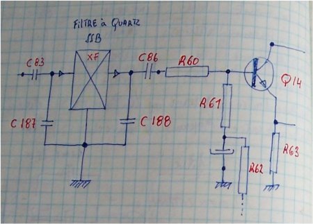
Ths crystal oscillator Q12 is operating at 10.695 MHz in the AM/FM/USB mode, and 10.692 MHz in the LSB mode, controlled by the Crystal, X3. This signal is =1; in the AM and FM modes of transmission, fed to the IC3 to be mixed with the first TX local oscillator frequency and result in 27 MHz transmitter frequencies, and =2; in the SSB modes of transmission, modulated through the balanced rnodulator IC4 with the audio output signal from the microphone amplifier, IC5. Thé resultant output of the balanced modulator is a double sideband. suppressed carrier signal. The crystal filter. XF, pass band is restricted to 3.5 kHz so that it allows only one sideband to pass through its output terminals, either USB or LSB mode, depending upon the Mode Selector switch selection. The exact frequency of which was determined by the Channel Selector switch selection and the PLL circuitry, us previously outlined, the resultant frequency, therefore, that is fed to the RF amplifier in IC3, is the channel frequency on the channel selected [channel 1 through 120 over 26.965 to 28.305 MHz]. The 27 MHz RF amplifier output is coupled to RF predriver transistors, Q7, 8. throuqh T4, 5. The predrivers serve to isolate the oscillator and mixer stages from the output amplifiers, and at the same time provide a certain amount of power gain. Q8 output is applied to the base input of Q9, the RF driver stage and in turn to the Q10, the RF power output stage of the transmitter. These stages amplify the 27 MHz RF signal resulting in an output at L13 of 5 watts in the AM, 6 watts in FM mode, and 13 watts PEP [peak envelope power] in the SSB mode.
Modulation Circuit
AM: The microphone feeds voice audio through Q701 on PTSW072 to the power audio IC IC5, and finally to collectors of Q9 and final RF power amplifier Q10 through T16, thereby amplitude modulating The carrier in AM transmission.
FM: In the FM mode, IC5 output is led to the anode of the FM modulating Variable capacitor D5 (also involved for ‘Tune’ control) in circuit board assembly PTOS006, varying its bias to change parallel cspacitance to X2, X3, or X4, finally giving deviation to PLL output frequency. SSB: The IC5 output is directly fed to the balanced modulator IC4, resulting in suppressed carrier double side band, which is in turn supplied to the crystal filter to carrier removal. ALC: An audio ALC [automatic Ievel control] voltage derived from the audio signal at Q35 is fed to IC5 îo control the output of audio amplifier to prevent overmodulation, in the AM or FM transmission, the output of Q35 is led to Q37 and is used to contro the output of T16. whereas in the SSB transmit mode, the output of Q35 is fed to Q38 and is connected to the primary side of T16. This being due to the fact that the output of IC5 [modulation signal] is fed [to modulate the RF signal] from the secondary side of T16 in the AM or FM mode, and from the primary side of T16 in the SSB mode of transmission.
The transceiver is also equipped with the RF ALC circuit utilizing the RF output induced at the input of L12 [in the SSB mode only). The minus voltage detected through D8 is applied to the DC plus bias circuit [pin number 7 of IC3, TX mixer] thus reducing the gain of the TX mixer as high level RF signal is observed at L12. This circuit is disabled in the AM or FM mode of transmission. In summary. the ALC circuit [both audio and RF] accomplishes very important function, not only preventing overmodulation, but in the view of harmonic and spurious suppression [especially in the SSB transmit mode].
Antenna Transmission Line
The lowpass filter between the antenna and collector of Q10 serves to pass the 27 MHz signals, attenuating higher frequency signals- It also acts to match the antenna impedance to the output impedance of the transmitter output stage, this nominally being 50 Ohm.
Receiver
Thé RF signal, at a frequency between 26.965 to 28.305 MHz, feeds from the antenna through L13, 12, 11, and T7 to the 27 MHz RF amplifier Q20. Then the amplified output signal from Q20 is coupled through T9 to first mixer Q22 where it is beat with an injection signal from the VCO, IC2, through the VCO buffer Q2.
The frequency of the injection signal from IC2 depends on the channel being selected, as a signal of the 37 MHz range is programmed by the Channel Selector. The output of Q22 is therefore. 10.695 MHz in the AM/FM/USB modes, and 10.692 MHz in the LSB mode, the first intermediate frequency and is the result of the RF input and mixing of IC2 VCO signals.
In case of the AM or FM receive mode, this 10.695 MHz first IF signal is then fed to the second mixer, balanced D22 and D23. AIso fed to the second mixer is the second local oscillator signal, 10.24 MHz, from Q3. Mixing of these two signals result in a signal at a frequency of 455 kHz in T14. This is the second intermediaie frequency for AM or FM mode of reception. In AM mode, the 455 kHz signal passes through the ceramic bandpass filter CF, and fed 10 IF amplifiers Q27, 28, and 29, which include IF transformer T15. The output of Q29 is applied to Q25, the AM diode detecter, while in FM receiving mode, the 455 kHz signal amplified only through Q27 is led to FM demcdulating IC, IC3 on the PTOS006 through T4. Resultant demodulated audio is acheived from the IC pin =12 and input to AF gain control VR, VR1. In the SSB mode of reception, the signal obtained as a result of the mixing of the RF input and IC2 VCO signals, 10.695 MHz in the USB, and 10.692 MHz in the LSB mode, is not converted down to lower iniermediate frequency, but is passed through the crystal filter, XF, and fed to the SSB IF amplifiers, Q14, 16, and 17, which includes T11, and 12. The signal at the secondary side of T12 is fed to Q19, the product SSB detector and beat with the BFO [béat frequency oscillator] signal from the Q12 and finally rectified to audio frequency signal.
The audio signal output from detectors (for AM [D25], FM [IC2], and SS3 [Q19]), is passed through the A F Gain Control, VR1, lo the input of the audio amplifier, IC5. The audio output is transformer coupled to the internal speaker, or to an external speaker through External Speaker jack, J3.
Squelch
Q32, 33, and 34 are the squelch amplifier transistors. At low [or no] signal levels Q34 collector conducts to ground and its output connected to pin
number 6 of IC5 results in no signal output from the audio amplifier. As the incoming RF signal increases it results in opening up the AF amplifier andoutput is activated. The point at which Q34 cuts off is determined by setting of the Squelch Control, VR2.
Noise Blanker Circuit
Noises contained in the output from Q-20 pass C-112 and fed to Q-23, noise amplifier. The noises are rectified by D-20 and D-21 to turn on Q-24 (FET) which in turn turns on Q-25 and Q-26. This causes the IF signal (10.695 and 10.692 MHz) at T-10 to short out to ground through C-21 and Q-26, during the presence of the noise impulses, virtually blanking out the noises from the audio output (The period during which che receiver is silenced is of such short duration of 10 microsecond or less that there is virtually no audible effect on the output.)
'Tune' Circuit
The tune control facility allows between-channel operation by shirting both the transmit and receive frequencies 4.5 kHz above or below the assigned channel frequency. The active elements of this circuit are the variable-capacitance diodes D-4, D-5 and VR-2 (front panel). The capacitance of both diodes will vary in accordance with the bias level determined by VR-2 adjustment, thus increasing or decreasing the parallel capacitance to R-14 at Q-4 emitter through C-25, and the external capacitance to X-l, X-2 or X-3 (D-5) simultaneously.
Clarifier Circuit
The clarifier control operates only in the receive mode to change the receive frequency regardless of the transmitting frequency (though the transmitting frequency is affected by the Tune control). Another VR portion of the double VR pair VR-2 acts to vary the, plus bias voltage of D-301 on the 'Clarifier unit circuit board" , in the same manner as of the tune circuit. Thus, the frequency Q-4 oscillates will be pulled above (VR-2 rotated clockwise), or down (rotated counterclockwise) its normal frequency. D-301 is fixed biased when the unit is transmitting.
adjustment procedures
Test Equipment
The following test equipment are required for servicing:
1 A 50 ohm resistive antenna load, 20 W.
2 A frequency counter operable in the required frequency range.
3 A HF signal generator operable over 50 kHz to 60 MHz.
4 An
oscilloscope.
5 An
FM déviation meter.
6 A
digital voltmeter.
7 An
8 ohm 5 W résistive speaker load.
8 Two audio
signal generators, 10 Hz to 20 kHz.
9 An
RF voltmeter.
10 A
circuit tester, input impedance 20 kohm/V.
11 A regulated dc power supply.
12 Dummy microphone plugs, receive and transmit mode, wired as shown.
Transmitter Alignment
Connect test equipment to the unit as shown :
PLL Alignment (FTOS006)
1 Connect
frequency counter to TP-1 (or IC-1 pin # 3), through 1,000 pF
capacitor.
2 Adjust CT-1 for 10.240 MHz. Tolerance within +/- 50 Hz is acceptable.
Off-set frequency alignment (PTOS006 unless otherwise noted)
For adjusting frequency of X-l, X-2, X-3 the tune and clarifier circuits most be in off position
1 Connect frequency counter to TP-4, set to maximum range.
2 Set the Mode selector to USB.
3 Set the Band selector LO.
4 Adjust CT-2 for 20.105 MHz +/- 40 Hz.
5 Set the Band selector to MID
6 Adjust CT-3 for 20.330 MHz +/-40 Hz.
7 Set the Band selector to HI.
8 Adjust CT-4 for 20.555 MHz +/-40 Hz.
9 Set The Band selector to MID, the channel selector to (60)
10 Connect scope to TP-4.
11 Adjust T-l for maximum scope amplitude.
12 Connect frequency counter to TP-5 (PTBM059).
13 Adjust CT-5 (FTBM059) for 10.695 MHz +/- 50 Hz.LSB Off-set alignment
1 Set the Mode selector to LSB, the Band selector to LO.
2 Connect frequency counter to TP-4 (PTOS006).
3 Adjust CT-5 (PTOS006) for 20.1035 MHz +/- 40 Hz.
4 Connect frequency counter to TP-5 (PTBM059).
5 Adjust CT-4 for 10.692 MHz +/- 50 Hz.VCO alignment
1 Set the Band selector to LO, and the Channel selector to 1.
2 Connect digital voltmeter to TP-2 (+) .
3 Adjust core of VCO-unit-case to 3.6 V +/- 0.1 V.
4 Set the channel selector to 41, and the Band selector to MID.
5 AdjustVR-l for 3.7 V +/- 0.1 V.
6 Set the channel selector to 1, and the Band selector to HI (81 channel).
7 Adjust VR-2 for 3.8 V +/- 0.1 V.RF power amplifier alignment
1 Set the Band selector to LO and the channel selector to 1.
2 Set the Mode switch to USB.
3 Feed 2,400 Hz 10 mV audio to unit (use dummy microphone plug prewired) .
4 Adjust T-3 (PTOS006) and T-5 (PTBM058) for maximum scope display.
5 Set the Band selector to HI, and the channel selector to 40 (channel 120) .
6 Adjust T-2 (PTOS006) and T-4 (PTBM058) for maximum scope display.
Carrier Leakage Alignment (PTBM059)1 Set the channel selector to 60, the band selector to MID.
2 Feed 2,400 Hz 10 mV audio to unit.
3 Adjust T-6, L-ll. L-12 and L-13 for maximum output on RF wattmeter.
4 Remove test audio.
5 Adjust RV-4 and RV-5 for minimum leakageon scope.
Two-tone alignment
1 Feed 500 Hz and 2,400 Hz audio tones to the microphone input circuit at the same time. Use two audio signal generator sets with attenuators.
2 Adjust: both test audio levels by means of attenuators on the generators so that the scope presents wave figure like shown as "A" in the diagrams below.A. Properly adjusted transmitter.
B. Unequal tones — Adjust generator outputs to balance.
C. Excessive modulation — Adjust RV11 “counterclockwise”.
D. Final transistor incorrectly biased — Adjust RV 1
E. Undermodulation — Adjust RV11 clockwise
F. Similar to A but showing hum — Check for proper testing condition.
3 Adjust RV-11 to obtain 18 W PEP power output
AM RF power alignment
1 Set the Mode selector to AM.
2 Select the channel 60 (MID band) .
3 Adjust RV-8 for 5 W RF power output.
AM modulation alignment
1
Apply 2.400 Hz 7 mV audio to the unit microphone input.
2
Adjust RV-12 for modulation depth 80 %
3 Increase audio level to 70 mV.
4
Check modulation depth is now 90 %.
FM modulation alignment
1 Set the Mode switch to FM.
2 Apply 2,400 Hz 10 mV audio to modulation circuit. Use dummy microphone plug.
3 Connect deviation meter to antenna output on the unit.
4 Adjust RV-3 (PTOS006) to obtain 1.5 kHz deviation.
RF power meter alignment
1 Set the unit to AM.
2 Comparing the extemal RF power and the built-in meter, adjust RV-3 (PTBM059) for equal indication on the power meters.
Transmitter Alignment Connect test equipment to unit as shown :
AGC
1 Connect digital voltmeter to circuit board PTBM059 terminal # 15 (Q-20, Q-22 AGC input) and chassis ground.
2 Set the transceiver to channel 60 (MID band). 41 to 80
3 Set DX/Local switch to DX.
4 Adjust RV-8 for 2 V.
AM receiver sensitivity1 Set signal generator to 27.655 MHz with 1 kHz 30 % modulation.
2 Set channel selector to channel 60 (MID band).
3 Set mode selector to AM.
4 Adjust T-7, T-8, T-9, T-10, T-13, T-14 and T-15 for maximum audio output from speaker output terminals (across dummy speaker load).
Note. Keep generator output level as low as possible to avoid AGC action.
5 After completing above, rotate T-7 to decrease the audio by 2 dB.
Squelch
1 Set mode selector to AM.
2 Set signal generator to provide RF of 300 microvolt 1 kHz 30 % modulated, squelch control to the fully clockwise position.
Avis, commentaires, suggestions
: Cliquez
ici
 |
 |
 |
Copyright Daviken 2003 - 2019